

| 09:00-10:40 | Th1: Adsorbate and interface dynamics |
| 10:40-11:20 | Coffee break |
| 11:20-13:00 | Th2: STM-IETS and beyond |
| 13:00-15:30 | Lunch break (on your own) |
| 15:30-16:40 | Th3: Molecular films and 2D materials |
| 16:40-17:20 | Coffee break |
| 17:20-19:00 | Th4: Tip-enhanced vibrational spectroscopies |
| 20:30-23:00 | Conference dinner at Cofradía Vasca de Gastronomía, Old Town |
Chair: P. Jelínek, Prague, Czech Republic
Contributed talk
Plasmon-phonon dynamics at GaP/Si(001) interfaces
1Nano-characterization Unit, National Institute for Materials Science, Tsukuba, Japan
2Department of Physics and Materials Science Center, Philipps-Universität Marburg, Germany
3Department of Physics and Astronomy, University of Pittsburgh, USA
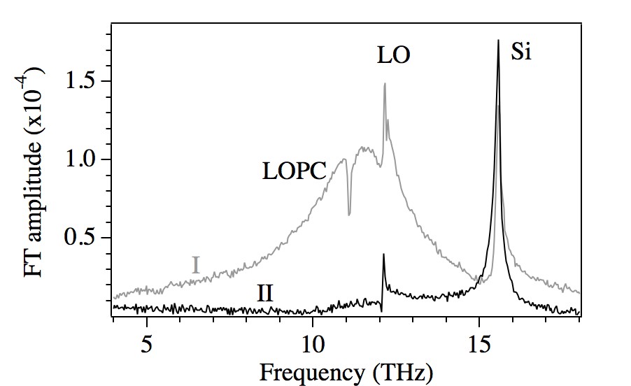
Charge carriers in impurity-doped semiconductors can behave collectively as a plasma oscillation. In polar semiconductors the plasma couples with the lattice polarization of the longitudinal optical (LO) phonons, resulting in LO phonon-plasmon coupled (LOPC) modes. The LOPC modes in III-V semiconductors can also be observed as coherent oscillations in the time domain. Monitoring the coherent LOPC mode by means of pump-probe reflectivity measurements can give a good measure of the chemically doped and photoexcited carriers, since the frequency and the dephasing rate depends crucially on the carrier type and density. Here we evaluate the charged carriers at the buried interface of GaP/Si(001) by means of coherent phonon spectroscopy. Lattice-matched GaP layers free from dislocations, staking faults or twins can be grown on exact Si(001) substrate by metal organic vapour phase epitaxy (MOVPE) [1]. Anti phase domains (APDs) are still unavoidable, however, and their boundaries consisting of the "wrong" bonds are expected to affect the interfacial electronic states crucially. Figure 1 compares the FT spectra of the anisotropic reflectivity changes of GaP/Si(001) samples with and without anti-phase domains (APDs). The GaP/Si sample without APDs (II) features oscillations due to the optical phonon of Si substrate at 15.6 THz and the LO phonon of GaP at 12 THz. The GaP/Si sample with APDs (I), by contrast, exhibits a prominent broad peak appears, whose frequency downshifts with increasing pump density. Similar mode was observed also for n-type GaAs(001) and assigned as the coherent LO phonon coupled with photoexcited multicomponent plasma [2]. The efficient generation of coherent LOPC mode for the interface sample with APDs indicates the presence of the surface built-in electric field, like for n-doped GaAs, in spite that the GaP film is nominally undoped. Our observation suggests that the boundaries of APDs act as donors.

Figure 1: FT spectra of anisotropic reflectivity changes of GaP/Si(001) samples with APDs (I) and without APDs (II) pumped at different pump densities.
[1] A. Beyer et al., J. Appl. Phys. 111, 083534 (2012)
[2] A. K. Basak et al., Phys. Rev. B 91, 125201 (2015)