

Poster
The butterfly effect – modelling STM imaging on Si/Ge(001):H
1Centro de Física de Materiales CSIC-UPV/EHU, Paseo Manuel de Lardizabal 5, 20018 San Sebastián, Spain
2Center for Nanometer-Scale Science and Advanced Materials, NANOSAM, Jagiellonian University, Reymonta Str. 4, PL 30-059, Krakow, Poland
3Donostia International Physics Center, DIPC, Paseo Manuel de Lardizabal 4, 20018 San Sebastián, Spain
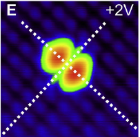
Dangling bond arrays on Si/Ge(001):H substrates can be patterned with atomic precision very rapidly and exhibit complex and rich physics making them interesting from both technological and fundamental physics perspectives [1,2]. But the complex behavior makes Scanning Tunneling Microscopy (STM) imaging difficult to interpret. In particular, an interesting symmetric empty-state image, the "butterfly", has so far eluded precise explanation.
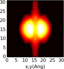
We propose a simple model to explain the "butterfly" - that (1) the electron-phonon coupling is strong enough to quickly sample several degenerate microscopic states and that (2) the transition rate out of a specific microscopic state is proportional to the STM current in that state. This model reproduces experimental STM images very well for both Si and Ge. Furthermore, based on our model, we propose a method to actively switch these microscopic states with high selectivity.


Figure 1: Empty-state image of a nearest-neighbor pair of dangling bonds on the Si(001):H surface (left, reproduced from [2]) and simulated image based on our proposed model (right).
[1] R. A. Wolkow et al., Field-Coupled Nanocomputing, Springer (2014)
[2] M. Kolmer et al., Appl. Surf. Science 288, 83 (2014)