Poster
Asymmetrical tunneling spectroscopy of close-spaced dangling-bond pairs on Si(001):H
1Centro de Física de Materiales CSIC-UPV/EHU, Paseo Manual de Lardizabal 5, 20018 Donostia-San Sebastián, Spain
2Centre for Nanometer-Scale Science and Advanced Materials, NANOSAM, Faculty of Physics, Astronomy and Applied Computer Science, Jagiellonian University, Krakow, Poland
3Donostia International Physics Center, Paseo Manual de Lardizabal 4, 20018 Donostia-San Sebastián, Spain
4IKERBASQUE, Basque Foundation for Science, E-48013, Bilbao, Spain
We present a combined experimental and theoretical study of the electronic properties of close-spaced dangling-bond (DB) pairs on a hydrogen-passivated Si(001):H p-doped surface. Two types of DB pairs are considered, called "cross" and "line" structures.
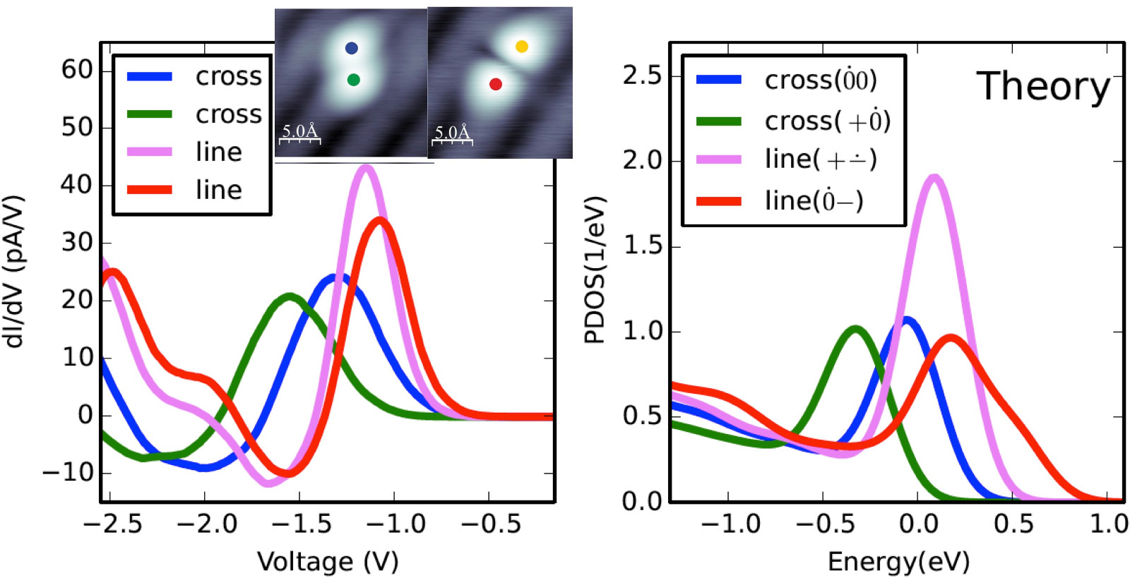
Our scanning tunneling spectroscopy (STS) data show that, although the spectra taken over different DBs in each pair exhibit a remarkable resemblance, they appear shifted by a constant energy that depends on the DB-pair type. This spontaneous asymmetry persists after repeated STS measurements. By comparison with density functional theory (DFT) calculations, we demonstrate that the magnitude of this shift and the relative position of the STS peaks can be explained by distinct charge states for each DB in the pair, and how these charge states are modified by the presence of the scanning tunneling microscopy (STM) tip and the applied bias. Our results indicate that, using the STM tip, it is possible to control the charge state of individual DBs in complex structures, even if they are in close proximity. This is observation might have important consequences for the design of electronic circuits and logic gates based on DBs at silicon surfaces.
Figure 1: Left panel: STS spectra of different DBs on different types of DB-pairs (STM images in the insets). Right panel: calculated PDOS for each type of pair assuming that transition to a neutral charge-state takes place when a positively-charged DB is imagined with a sufficiently negative bias (energies relative to the valence band top of the Si(001):H ).